Thursday 24 November 2011

Fixed Bias Transistor Circuits


Few Points:
  1. Two batteries vBB and VCC used
  2. VBB gives potential to base terminal through RB.
  3. VCC  supplies power to the collector through RC.
  4. Base resistance RB  of the order of hundred kilo ohm
  5. Collector resistance RC of the order of kilo ohm.
Aim: To find dc base current IB, IC, VCE and I
For this purpose, we are going to convert  above circuit in electrical equivalent circuit. For making calculation easy, we divide this circuit in two part, (i) Input Part and (ii) Output Part

(I)  Input Part:
Applying KVL:
We get, VBB = IBRB + VBE
Or  IB = ( VBB – VBE )/ RB
For Silicon Transistor, VBE = 0.7 V and For Ge Transistor, VBE = 0.3 V

(ii) Output Part:

Applying KVL again,
VCE = VCC – IC RC
We know that,  IC = β IB

Stability Factor (S) = ( 1 + β )/(1 – β d IB / d IC)
And  in fixed biased, IB is independent of IC.
Hence, S = ( 1+ β )
It means collector current (IC) increases ( 1 + β ) times as much as ICO .


Biasing of Transistor:


Need of Biasing:
  • The proper flow of zero signal collector current and the maintenance of proper collector emitter voltage during the passage of signal is called the transistor biasing.
  • It is essential for faithful amplification.
If the transistor is not biased properly, It would be
  • Work inefficiently
  •  Produce distortion in the output signal.
Keep in Mind:
  • Input side should be in Forward Biased
  • Output side should be in Reverse Biased
  • Base Resistance RB >>RC
There are some transistor biasing circuits:
  1. Fixed Bias
  2. Potential Divider Bias
  3. Two Supply Emitter Bias
  4. Emitter – Feedback Bias
  5. Collector Feedback Bias
  6. Collector – and Emitter – Feedback Bias


Wednesday 23 November 2011

Troubleshooting of a Transistor circuit


Troubleshooting  a circuit:
  • 1.       Measure the Vce.
  • 2.       When troubles come, they are usually big troubles like shorts or opens.
  • 3.       Short: when  devices damaged, solder splashes across resistors.
  • 4.       Open: when components burn out.
  • 5.       These troubles produce large changes in voltages and currents

 Welcome to S2P Group. For more information. connect to study2placement.blogspot.com
Cause of these troubles:
1.       Trouble in the power supply
2.       An open lead between the power supply and the collector resistor
3.       An open collector resistor and so on.
4.       Open base resistor

Trouble
VB, V
VC,V
Remarks
None
0.7
12
No trouble
RBS
15
15
Transistor Blown
RBO
0
15
No Base or Collector Current
RCS
0.7
15
Check RC and Supply  connection
RCO
0.7
0
           “
No VBB
0
15
Check supply and lead
No VCC
0.7
0
          “

For Example:


If VBB=15V, RB=470kohm, RC=1k ohm, VCC=15 V, current gain= 100

We assume ideal condition. Suppose RB= 1 M ohm, then base current would be 15 uA. Here RB is 470 k ohm nearly half of the 1M ohm. Hence base current would be double, i.e 30 uA. And current gain is 100. So collector current would be 3 mA. When it flows through 1 kohm resistor, it produces a voltage drop of 3 V. So, VCE would be 12 V, or else there is something wrong in this circuit.

Projects Based on C++

There are some useful projects for Computer Science students:


Monday 21 November 2011

Electronic mosquito repeller


Here is the circuit diagram of an ultrasonic mosquito repeller.The circuit is based on the theory that insects like mosquito can be repelled by using sound frequencies in the ultrasonic (above 20KHz) range.The circuit is nothing but a PLL IC CMOS 4047 wired as an oscillator working at 22KHz.A complementary symmetry amplifier consisting of four transistor is used to amplify the sound.The piezo buzzer converts the output of amplifier to ultrasonic sound that can be heard by the insects.
Circuit diagram :

Main Parts Used:
IC CD4047 ( a Phased Lock Loop) - 1
4 Transistor ( 2 NPN (SL100) and 2 PNP (SK100))
Capacitors ( 4.7 nF, 22uF 16V)
10K Potentiometer - 1
Welcome to S2P Group. For more details: www.study2placement.blogspot.com

Note

  • Assemble the circuit on a general purpose PCB.
  • The circuit can be powered from 12V DC.
  • The buzzer can be any general purpose piezo buzzer.
  • The IC1 must be mounted on a holder
  • R1 and C1 are deciding the frequency of Ocillator.


How does the Timer 555 work

Block diagram for the 555 timer is given in fig.


Main Parts of 555 Timer:

  • Two comparators (simply Op-Amp)
  • An R-S Flip-flop
  • Two Transistors
  • A Resistive networks consisting three equal resistors and acts as a voltage divider


Working:
In most applications, the control pin is not used, so that the control voltage equals +2Vcc/3 .
Output of comparator 1 is applied to set (S) input of the flip-flop. Whenever the threshold voltage exceeds the control voltage, comparator 1 will set the flip-flop and its output is high. A high output from the flip-flop saturates the discharge ttransistor and discharge the capacitor connected externally to pin 7. The complementary signal out of the flip-flop goes to pin 3, the oputput. The output available at pin 3 is low. Even if the voltage at the threshold input falls below +2Vcc/3, comparator 1 cannot cause the flip-flop to change again. It means that the comparator 1 can only force the flip-flop's output high.
To change the output of flip-flop to low, the voltage at the trigger input must fallbelow +Vcc/3. When this occurs, comparator 2 triggers the flip-flop, forcing its output low. The low output from the flip-flop turns the discharge transistor off and forces the power amplifier to output a high.

Note: When control input is not in use, a 0.01 uF capacitor should be connected between pin 5 and ground to prevent noise coupled onto this pin from causing false triggering.

How a Capacitor Works


An electrical capacitor is made of two small conductive plates separated by what is called a dielectric, which effectively insulates the two plates and stops any current from being transferred between the plates themselves. Instead, the two plates are connected through a circuit. When the circuit is taken out, the plates store the electrical current because it can't flow between the plates.

The way a capacitor works is like a water storage tank with a shut-off valve if it gets too full. As electrical current enters the capacitor, the capacitor lets it pass through unaffected. However, the more current flows into the capacitor, the quicker it "fills." This then triggers the capacitor's shut-off mechanism, preventing electrical current from exiting and redirecting the flow to a grounding current.


Capacitor Coding:


How a Capacitor works in a Fan
One use is to provide phase shift in one of the motor's windings. This is either called a "capacitor start" motor, or a "capacitor start / capacitor run" motor.
Since a motor must have a rotating magnetic field to produce rotation of the rotor, the capacitor, produces a phase shift in one winding so it lags and produces a lagging field compared to the other winding. This time lag will then cause a rotating force or torque on the rotor...thus rotating the rotor and making a motor.

How Inductor works


When a current flows into an inductor, it doesn't go round and round and round the turns, taking its time to get to the other end. An inductor wound with 100 feet of wire behaves nothing like a 100 foot wire. Why?

It's because when the current begins flowing, it creates a magnetic field. This field couples to, or links with, the other turns. The portion of the field from one turn that links with the others is the measurable quantity called the coefficient of coupling. For a good HF toroid, it's commonly 99% or better; solenoids are lower, and vary with aspect ratio. The field from the input turn creates a voltage all along the wire in the other turns which, in turn, produce an output current (presuming there's a load to sustain current flow). Consequently, the current at the input appears nearly instantaneously at the output. Those who are physics oriented can have lots of fun, I'm sure, debating just how long it takes. The field travels at near the speed of light, but the ability of the current to change rapidly is limited by other factors.The coupling of fields from turn to turn or region to region is what brings about the property of inductance in the first place.
One of the characteristics that make inductors useful is that their reactance (opposition to AC current) increases with frequency. (unlike a capacitor, for which the reactance decreases with frequency).

Thus inductors when combined with capacitors become useful when you want to make filters that let only chosen frequencies through, such as cross-overs for speakers or tuner circuits in radios.

Sunday 20 November 2011

50% DUTY CYCLE OSCILLATOR


For  a  50%  duty  cycle,  the  resistors  RA    and  RB    may  be connected as in Figure 14. The time period for the output high is the same as previous, t1  = 0.693 RA  C.
For the output low it is t2  =
Thus the frequency of oscillation is
Note that this circuit will not oscillate if RB  is greater than 1/2 RA   because the junction of RA   and RB   cannot bring pin 2 down to 1/3 VCC  and trigger the lower comparator.
ADDITIONAL INFORMATION
Adequate power supply bypassing is necessary to protect associated circuitry. Minimum recommended is 0.1µF in parallel with 1µF electrolytic. Lower  comparator  storage  time  can  be  as  long  as  10µs when pin 2 is driven fully to ground for triggering. This limits the monostable pulse width to 10µs minimum. Delay time reset to output is 0.47µs typical. Minimum reset pulse width must be 0.3µs, typical. Pin  7  current  switches  within  30ns  of  the  output  (pin  3) voltage.


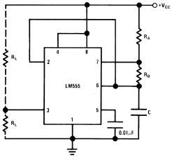
LINEAR RAMP using 555


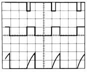
When the pull up resistor, RA, in the monostable circuit is replaced  by  a  constant  current  source,  a  linear  ramp  is generated. Figure 1 shows a circuit configuration that will perform this function.


Welcome to S2P Group.

Figure 2 shows waveforms generated by the linear ramp.
The time interval is given by:

VBE  . 0.6V For more informations: www.study2placement.blogspot.com
VCC  = 5V
TIME = 20µs/DIV.
R1  = 47kΩ
R2  = 100kΩ
RE  = 2.7 kΩ
C = 0.01 µF


PULSE POSITION MODULATOR


This application uses the timer connected for astable operation, as in Figure 1, with a modulating signal again applied to the control voltage terminal. The pulse position varies with the modulating signal, since the threshold voltage and hence the time delay is varied. Figure 2 shows the waveforms generated for a triangle wave modulation signal.


VCC  = 5V
TIME = 0.1 ms/DIV.
RA  = 3.9kΩ
RB  = 3kΩ
C = 0.01µF

PULSE WIDTH MODULATOR


When the timer is connected in the monostable mode and triggered  with  a  continuous  pulse  train,  the  output  pulse width can be modulated by a signal applied to pin 5. Figure 1  shows  the  circuit,  and  in  Figure  2  are  some  waveform
examples.
VCC  = 5V
TIME = 0.2 ms/DIV.
RA  = 9.1kΩ
C = 0.01µF


ASTABLE OPERATION


If the circuit is connected as shown in Figure 1  (pins 2 and 6 connected) it will trigger itself and free run as a multivibrator. The external capacitor charges through RA   + RB   and discharges through RB. Thus the duty cycle may be precisely set by the ratio of these two resistors.

In this mode of operation, the capacitor charges and discharges between 1/3 VCC   and 2/3 VCC. As in the triggered mode, the charge and discharge times, and therefore the frequency are independent of the supply voltage. Figure 2 shows the waveforms generated in this mode of operation.
VCC  = 5V
TIME = 20µs/DIV.
RA  = 3.9kΩ
RB  = 3kΩ
C = 0.01µF
The charge time (output high) is given by:
t1  = 0.693 (RA  + RB) C
And the discharge time (output low) by:
t2  = 0.693 (RB) C
Thus the total period is:
T = t1  + t2  = 0.693 (RA  +2RB) C
The frequency of oscillation is: 


It may be used for quick determination of these RC values.
The duty cycle is: 


MONOSTABLE OPERATION using 555


In this mode of operation, the timer functions as a one-shot (Figure 1). The external capacitor is initially held discharged by a transistor inside the timer. Upon application of a negative trigger pulse of less than 1/3 VCC  to pin 2, the flip-flop is set which both releases the short circuit across the capacitor and drives the output high. For More information: www.study2placement.blogspot.com


The voltage across the capacitor then increases exponentially for a period of t = 1.1 RA  C, at the end of which time the voltage  equals  2/3  VCC.  The  comparator  then  resets  the flip-flop which in turn discharges the capacitor and drives the output to its low state. Figure 2 shows the waveforms generated in this mode of operation. Since the charge and the threshold level of the comparator are both directly proportional to supply voltage, the timing interval is independent of supply.


Welcome to S2P Group.

VCC  = 5V
TIME = 0.1 ms/DIV.
RA  = 9.1kΩ
C = 0.01µF

During the timing cycle when the output is high, the further application of a trigger pulse will not effect the circuit so long as the trigger input is returned high at least 10µs before the end of the timing interval. However the circuit can be reset  during this time by the application of a negative pulse to thereset terminal (pin 4). The output will then remain in the  lowstate until a trigger pulse is again applied.When the reset function is not in use, it is recommended that it  be  connected   to  VCC    to  avoid  any  possibility  of  false triggering. Figure  3  is  a  nomograph  for  easy  determination  of  R,  C values for various time delays.
NOTE: In monostable operation, the trigger should be driven high before the end of timing cycle.


LM555 Timer


The LM555 is a highly stable device for generating accurate time delays or oscillation. Additional terminals are provided for triggering or resetting if desired. In the time delay mode of operation, the time is precisely controlled by one external resistor and capacitor. For astable operation as an oscillator, the  free  running  frequency  and  duty  cycle  are  accurately controlled with two external resistors and one capacitor. The circuit may be triggered and reset on falling waveforms, and the output circuit can source or sink up to 200mA or drive TTL circuits.

Pin 1: Grounded Terminal: All the voltages are meas­ured with respect to this terminal.

Pin 2: Trigger Terminal: This pin is an inverting input to a comparator that is responsible for transition of flip-flop from set to reset. The output of the timer depends on the amplitude of the external trigger pulse applied to this pin.

Pin 3: Output Terminal: Output of the timer is avail­able at this pin. There are two ways in which a load can be connected to the output terminal either between pin 3 and ground pin (pin 1) or between pin 3 and supply pin (pin 8). The load connected between pin 3 and ground supply pin is called the normally on load and that connected between pin 3 and ground pin is called the normally off load.

Pin 4: Reset Terminal: To disable or reset the timer a negative pulse is applied to this pin due to which it is referred to as reset terminal. When this pin is not to be used for reset purpose, it should be connected to + VCC to avoid any possibility of false triggering.

Pin 5: Control Voltage Terminal: The function of this terminal is to control the threshold and trigger levels. Thus either the external voltage or a pot connected to this pin determines the pulse width of the output waveform. The external voltage applied to this pin can also be used to modulate the output waveform. When this pin is not used, it should be connected to ground through a 0.01 micro Farad to avoid any noise problem.

Pin 6: Threshold Terminal: This is the non-inverting input terminal of comparator 1, which compares the voltage applied to the terminal with a reference voltage of 2/3 VCC. The amplitude of voltage applied to this terminal is responsible for the set state of flip-flop.
For More information: www.study2placement.blogspot.com
Pin 7 : Discharge Terminal: This pin is connected internally to the collector of transistor and mostly a capacitor is connected between this terminal and ground. It is called discharge terminal because when transistor saturates, capacitor discharges through the transistor. When the transistor is cut-off, the capacitor charges at a rate determined by the external resistor and capacitor.
Welcome to S2P Group
Pin 8: Supply Terminal: A supply voltage of + 5 V to + 18 V is applied to this terminal with respect to ground (pin 1).


Applications

  • Precision timing
  • Pulse generation
  • Sequential timing
  • Time delay generation
  • Pulse width modulation
  • Pulse position modulation
  • Linear ramp generator


UM66TXXL series Musical IC


MELODY INTEGRATED CIRCUIT

DESCRIPTION
The   UTC   UM66TXXL   series   are   CMOS   LSI designed for using in door bell,  telephone  and toy
application.  It  is  an  on-chip  ROM  programmed  for musical     performance.     Produced     by     CMOS
technology,  the  device  results  in  very  low  power consumption.   Since   the   UTC   UM66TXXL   series
include oscillation circuits a compact melody module can   be   constructed   with   only   a   few   additional
components.

FEATURES

  • 64-Note Rom memory consumption
  • Dynamic speaker can be driven with external NPN transistor
  • OSC resistor hold mode
  • Power on reset: melody begins from the first note
  • Built in level hold mode


FUNCTIONAL DESCRIPTION

OSCILLATOR CIRCUIT
The oscillator frequency is used as a time for tone and beat generators. Its accuracy affects the quality of the music.


TONE GENERATOR
Tone Frequencies are oscillator frequencies-M, where m is any even number from 64 to 256. Within a melody
14C scales can be selected including Pause code and End code. The tone generator is a programmed divider, The Range of Scales is from “C4” to “C6” and range of frequency varies from 258Hz to 23768Hz.

RHYTHM GENERATOR
The rhythm generator is also programmed dividers. It contain 15 available rhythms as
follows:1/4,1/2,3/4,1,1-1/4,1-1/2,1-/3/4,2,2-1/4,2-1/2,2-/3/4,3,3-1/4,3-1/2,3-/3/4.Four rhythms can be selected from these.

MELODY ROM
The Mask Rom can memorize 64 notes with 6 bit.4 bits are used for controlling the scale code and 2 bits are used for controlling the rhythm code.

TEMPO GENERATOR
There are 15 available tempos in the UTC UM66T series. The 15 tempos are:128,137,148,160,175,192,213, 240 , 274, 320,480,640,960,1920 J/minute.


BPW77 as Phototransistor


Silicon NPN Phototransistor 

DESCRIPTION
BPW77 is a silicon NPN phototransistor with high radiant
sensitivity in hermetically sealed TO-18 package with base
terminal and glass lens. It is sensitive to visible and near
infrared radiation.

FEATURES
• Package type: leaded
• Package form: TO-18
• Dimensions (in mm): Ø 4.7
• High photo sensitivity
• High radiant sensitivity
• Suitable for visible and near infrared radiation
                • Fast response times
                • Angle of half sensitivity: Ï• = ± 10°
                • Base terminal connected
                • Hermetically sealed package
                • Lead    (Pb)-free    component    in    accordance RoHS 2002/95/EC and WEEE 2002/96/EC

APPLICATIONS
• Detector in electronic control and drive circuits

CXA1619BM/BS a FM/AM radio IC


CXA1619BM/BS is a one-chip FM/AM radio IC designed for radio-cassette tape recorders and
headphone tape recorders, and has the following functions.

Features
• Small number of peripheral components.
• Low current consumption (VCC=3 V)
For FM : ID=5.8 mA (Typ.)
For AM : ID=4.7 mA (Typ.)
• Built-in FM/AM select switch.
• Large output of AF amplifier.
EIAJ output=500 mW (Typ.) when
VCC=6 V, load impedance 8 Ω
Function
FM section
• RF amplifier, Mixer and OSC
(incorporating AFC variable capacitor).
• IF amplifier
• Quadrature detection
• Tuning LED driver
AM section
• RF amplifier, Mixer and OSC (with RF AGC)
• IF amplifier (with IF AGC)
• Detector
• Tuning LED driver
AF section
• Electronic volume control


Structure
Bipolar monolithic IC
Recommended Operating Conditions
Supply voltage                VCC            2 to 7.5         V (CXA1619BM)
                              VCC            2 to 8.5         V  (CXA1619BS)

Tuesday 15 November 2011

Mobile robot with sonar scanner


Robot uses stepper motor to rotate the sonar sensor and it covers 180 degree. Each 45 degree, a sample is taken. There is a LED display which works like radar, and shows the detected obstacles.
Moreover, Robot can switch to remote control mode. So,we can simply control the motion and get samples using RF transmitter.

Circuit Diagram:

Download Source Code of Micro controller using C
                                         

Infrared entry alert door


An IR transmitter and IR receiver placed at either side of a doorway sends and receives IR stream. If the beam is broken, a buzzer will beep or a relay will trigger. Please read "readthis!.txt" for all information.
Welcome to S2P Community.
Circuit Diagram:
Transmitter:

Receiver:

Everything included, source, assembler, programmer, and Receiver and Emitter datasheets in docs folder.


Saturday 5 November 2011

Testing semiconductors with multimeters


Before building any circuit is it a good idea to test every semiconductor you plan to use in the project. This a good practice especially when reusing components from old appliances. This short tutorial describes common procedures for testing of Si and Ge signal and rectifier diodes, Zener diodes, LEDs, Bipolar and MOSFET transistors for common failures like shorts, leaks and opens.

Testing signal and rectifier diode junctions

A regular signal or rectifier diode should read a low resistance on an analog ohmmeter (set on the low ohms scale) when forward biased (negative lead on cathode, positive lead on anode) and nearly infinite ohms in the reverse bias direction. A germanium diode will show a lower resistance compared to a silicon diode in the forward direction. A bad diode will show near zero ohms (shorted) or open in both directions.
1n4007 diode
Note: often, analog multimeters have the polarity of their probes reversed from what you would expect from the color coding. Many of them will have the red lead negative with respect to the black one.
On a digital multimeter, using the normal resistance ranges, this test will usually show open for any semiconductor junction since the meter does not apply enough voltage to reach the value of the forward drop.
Fortunately almost every digital multimeter will have a diode test mode. Using this mode, a silicon diode should read a voltage drop between 0.5 to 0.8 V in the forward direction (negative lead on cathode, positive lead on anode) and open in reverse. For a germanium diode, the reading will be lower, around 0.2 - 0.4 V in the forward direction. A bad diode will read a very low voltage drop (if shorted) or open in both directions.
Note: small diode leaks in the reverse bias direction are rare, but they will often go unnoticed when using the diode test mode on the majority of digital multimeters. To make sure the diode is good, you should make one more measurement: using a high ohm range (2Mohm or higher) on your DMM, place the negative lead on the anode and the positive lead on the cathode. A good Si diode (the most common type of diode in today's circuits) will usually read infinite ohms. An older Ge diode may have a much higher level of reverse leakage current, so it may show a non-infinite value. When in doubt, try to compare the reading with measurements done on a good diode of the same type.

Testing Zener diodes

Simple Zener tester circuit
For a quick diagnosis, a Zener diode junction can be verified like a normal diode as described above. But, to test for reverse breakdown zener voltage, you will need a simple power supply with a voltage greater than the expected value and a high value resistor.
Connect a high value resistor (to limit the current to a safe value) in series with the zener diode and apply the voltage in the reverse direction across the diode (anode to the negative). The voltage measured across the diode will be the breakdown or zener voltage.

Testing LEDs

Simple LED tester circuit
LED diodes usually have a forward voltage drop too high to test with most multimeters, so you should use a similar circuit as the one described above.
Make sure to use a power supply greater than 3V and a suitable current limiting series resistor. A small current of 1-10 mA will be enough to light most LEDs when connected in the circuit.

Testing bipolar transistors

The assumption made when testing transistors is that a transistor is just a pair of connected diodes. Therefore it can be tested for shorts, opens or leakage with a simple analog or digital multimeter. Gain, frequency response, etc. tests can be made only with expensive specialized instruments, but in most cases a simple test is all you'll need when building simple circuits.
NPN transistor
Note: some power transistors have built in damper diodes connected across C-E and resistors connected across B-E which will confuse these readings. Also, a few small signal transistors have built-in resistors in series with the base or other leads, making this simple test method useless. Darlington transistors can also show unusual voltage drops and resistances. When testing a transistor of this type you will need to compare with a known good transistor or check the specifications to be sure.
To test a bipolar transistor with a digital multimeter, take it out of circuit and make the following measurements using the diode test mode:
  • Connect the red (positive) lead to the base of the transistor. Connect the black (negative) lead to the emitter. A good NPN transistor will read a junction drop voltage of 0.4V to 0.9V. A good PNP transistor will read open.
  • Leave the red meter lead on the base and move the black meter lead to the collector - the reading should be almost the same as the previous test, open for PNP and a slightly lower voltage drop for NPN transistors.
  • Reverse the meter leads and repeat the test. This time, connect the black meter lead to the base of the transistor and the red lead to the emitter. A good PNP transistor will read a junction drop voltage of 0.4V to 0.9V. A good NPN transistor will read open.
  • Leave the black meter lead on the base and move the red lead to the collector - the reading should be almost the same as the previous test, open for NPN and a slightly lower voltage drop for PNP transistors.
  • Place one meter lead on the collector, the other on the emitter, then reverse. Both tests should read open for both NPN and PNP transistors.
A similar test can be made with an analog VOM using the low ohms scale. Only 2 of the 6 possible combinations (the B-E and B-C junctions in forward bias) should show a low resistance (anywhere from 100 ohms to several Kohms) and none of the resistances should be near 0 Ohms.
If you read a short circuit (zero ohms or a voltage drop of zero) between two leads, or the transistor fails any of the tests described above, it is bad and must be replaced.
If you get readings that do not make sense, try to compare them with measurements done on a good transistor of the same type.
Some analog multimeters have their probe colors reversed since this makes the internal circuitry easier to design. So, it's a good idea to confirm and label the lead polarity of your instrument by making a few measurements in resistance (VOM) or diode test mode (DMM) using a known good diode. This will also show you what to expect for a reading of a forward biased junction.

Identifying the leads and polarity of unknown bipolar transistors

The type (PNP or NPN) and the lead arrangement of unmarked transistors can be determined easily using a digital or analog multimeter, if the transistor is seen as a pair of connected diodes. The collector and emitter can be identified knowing the fact that the doping for the B-E junction is always much higher than for the B-C junction, therefore, the forward voltage drop will be slightly higher. This will show up as a couple of millivolts difference on a digital multimeter's diode test scale or a slightly higher resistance on an analog VoltOhmMeter.
First make the a few measurements between various leads. Soon you'll identify a lead (theBase) that will show a forward voltage drop (on DMMs) or a low resistance (analog VOMs) combined with two other leads (the Emitter and Collector). Now that the Base is identified, observe carefully the voltage drops across B-E and B-C. The B-C junction will have a slightly less voltage drop (DMM) or a slightly lower resistance when using an analog ohmmeter.
Note: For every degree the transistor increases in temperature, the diode drops will decrease by a few millivolts. This change can be confusing when determining the B-E and B-C junctions. So, make sure you do not hold the transistor under test in your hand and leave enough time for it to cool down to room temperature after soldering!
If you arrived at this point, you already know the polarity of the transistor under test. If the negative lead (black lead connected to the COM on most digital multimeters) is placed on the Base when measuring the B-C and B-E voltage drops - you have a PNP transistor. Similarly - if the positive meter lead is placed on the base, you have a NPN transistor.
This procedure may sound complicated at first, but practicing on a few transistors with known leads will make things clearer in no time. It is a good habit to test every transistor before placing it into the circuit, as the datasheet is not always at hand, and misplacing the leads can have devastating results.

Testing MOSFETs

Field Effect Transistors are difficult to test with a multimeter, but "fortunately" when a power MosFet blows, it blows big time: all their leads will show in short circuit. 99% of bad MosFets will have GS, GD and DS shorted. In other words - everything will be connected together.
Note: When measuring a MosFet hold it by the case or the tab and don't touch the metal parts of the test probes with any of the other MosFet's terminals until needed. Do not allow a MosFet to come in contact with your clothes, plastic, etc. because of the high static voltages they can generate.
You'll know a MosFet is good when the Gate has infinite resistance to both Drain and Source. Exceptions to this rule are FETs with protection circuitry - they may act like there is a diode shunting GS - a diode drop for gate reverse bias. Connecting Gate to Source should cause the Drain to Source act like a diode. Forward biasing GS with 5V and measuring DS in forward bias should yield very low ohms. In reverse bias, it will still act like a diode.
Another simple test procedure: connect the multimeter's negative lead to the source of the MosFet. Touch the MosFet's Gate with the meter's positive lead. Move the positive probe to the Drain - you should get a low reading as the MosFet's internal capacitance on the Gate has now been charged up by the meter and the device is turned-on. With the meter's positive lead still connected to the Drain, touch the source and gate with your finger. The Gate will be discharged through your finger and the reading should go high, indicating a non-conductive device! This simple test is not fail proof, but it's usually adequate.

Friday 4 November 2011

Solar Powered USB Charger (phones, MP3 players etc)


This is my take on a already well documented little project. Very simple to make and a good introduction to electronics and solar powered stuff. Works just fine too. You need to generate 5-6V to charge a phone.
You will need:
Solar panels. I used 2 panels. (3V I think )
5V voltage regulator
USB female jack/connector
Insulated wire
Soldering Iron
Epoxy or hot glue

Step 1: Bits & Pieces


Gather together all your stuff. You need to make sure you know which side is top and which side is the bottom of the USB plug and the voltage regulator so that you solder the correct pins.
The regulator keeps the power output to 5v.

Step 2: A series of solar panels


A USB port from a computer puts out 5.5V for charging of phones and mp3 players. So you need to get about 5-6V from your solar panels. In this case I need to solder the solar panels in series in order to double the voltage output. (3V each panel).  Solder the positive of 1 panel to the negative of the other. (Its just like putting 2 batteries in a flashlight)

Step 3:  Solder it all together


Hook it all up!
The positive wire from the solar panels goes to the LEFT pin of the regulator. (mine is upside down in the photo)
The negative wire from the panels goes to the MIDDLE pin of the regulator and is also connected to the RIGHT pin of the USB plug. (Again, mine is upside down in the photos)
Then connect the last pin of the regulator to the other outside pin of the USB connector.
The 2 middle pins are not needed.
If you follow my pictures it will be OK....

Step 4: Glue


I used hot glue to hold it all together but an epoxy or duct tape will work fine.
Next time I would make it so that the 2 panels hinged in some way so that it could fold together.

It works!

 
Design by Wordpress Theme | Bloggerized by Free Blogger Templates | JCPenney Coupons